Raspberry Pi FWH, LPC, and SPI multi-tool
As I outlined in the fwhtool page, I encountered a case where I needed a cheap but reliable way to program FWH/LPC flash chips independently of the target computer. I was already using a Raspberry Pi Zero for its SPI capabilities, so since I realised I could squeeze LPC functionality onto the remaining GPIO pins, I decided to kill two birds with one stone and produce a neat solution that could handle all of these protocols without any fuss.
Software
First, let's have a look at the software side, to establish what we have to design around.
SPI functionality
In case you don't already know it, SPI on the Raspberry Pi is easy and can be achieved in a few simple steps.
- Set up a simple GNU/Linux environment you can remotely access on the device.
- Edit your
config.txtto contain the linedtparam=spi=on. This will present an SPI interface capable of two peripheral devices on pins 17 (3.3V), 19 (MOSI), 21 (MISO), 23 (SCLK), 24 (CE0), 25 (GND), and 26 (CE1). To my knowledge, the pinout is the same for all Raspberry Pi devices. - Set up the
flashromutility on the device, like you would when reprogramming the firmware on any other device. - You can now access the SPI interface with
flashrom -p linux_spi,dev=/dev/spidev0.X, whereXis either 0 or 1, referring to CE0/CE1.
Including a more user-friendly hardware interface to go alongside this will be described later in the article.
LPC/FWH functionality
This is trickier, as the Raspberry Pi has no hardware implementation of these protocol(s). I had to write my own program for it, using precisely-timed GPIO accesses. Thankfully, that work has already been done for you. The hard part will be designing some physical implementation that makes accessing these chips convenient. I will focus primarily on those utilising the PLCC32 socket, because that's the issue I was trying to solve initially. The pins of the Raspberry Pi that my program uses are described on the page for the software itself, but you'll see it again in schematics later in this article.
Hardware
I had never designed anything this complex before writing this article, so this was my first time using KiCad. (I was in a rush and mostly figured it out without checking any documentation, so please excuse any mistakes).
The gist of the issue is that we need to construct a PCB that attaches to the GPIO connector on the Raspberry Pi (like other conventional "hats") and exposes:
- A header to attach a SOIC-16 test clip, for SOIC-16 SPI chips.
- A header to attach a SOIC-8 test clip, for SOIC-8 SPI chips. We will wire these to separate Chip Enable pins, so we can access both separately.
- A PLCC32 socket, to put LPC/FWH chips. For reliability and ease of construction, I use a ready-made PLCC32 to DIP32 adapter, so that I don't have to do any complex soldering (this was my first time doing that seriously as well). This also makes the PLCC32 socket replaceable, in the event that the plastic around the edges snaps.
- An external power connector (and a switch to determine which rail to use) in order to allow the user to provide e.g. a bench power supply that can provide more current, mostly useful for SPI flash attached to boards without a diode (so power is fed to the chipset and other devices on the board as well).
I will be producing a schematic to follow, but no typical printed circuit board design (although I did experiment with making one). This is because in order to produce this quickly for my immediate uses, I wanted to work with a simpler and more readily accessible prototype board.
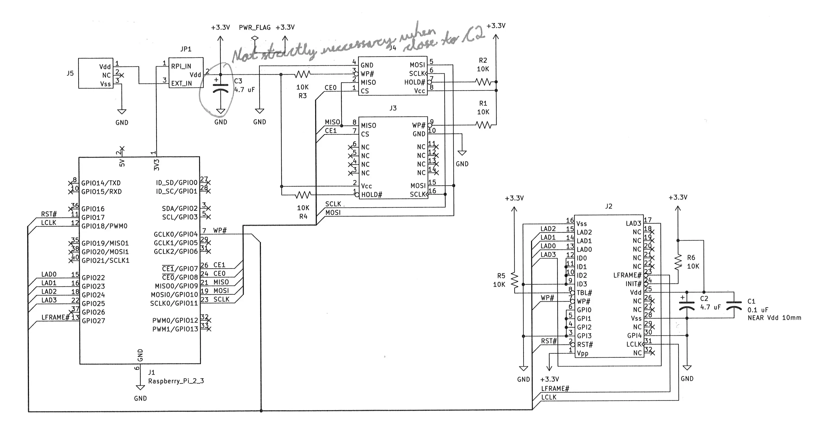
Figure 1. The first version of the schematic.
Figure 1 shows the schematic I produced while working on the prototype board, providing all of the features I specified above. Notice the two electrolytic and one ceramic decoupling capacitors; these are necessary, writing to most FWH/LPC chips without one for example will fail.
PLCC32 to DIP32
The 0.1 μF ceramic capacitor must be placed as close as possible to the LPC chip's Vdd. In order to do that successfully I had to get a bit creative...
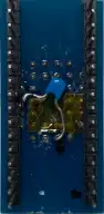
Figure 2. The underside of the PLCC32 to DIP32 adapter.
As you can see, the capacitor is placed directly onto the pins of the PLCC32 socket, insulated from the others with careful positioning of the legs and a piece of kapton tape.
This is tricky to solder. I myself needed help from someone more experienced (again, this was my first time), but one day I hope to be able to do it alone.
Main Programmer Board
With the adapter sorted, we can move on to the board between it and the Raspberry Pi. This will have a jumper switching between 3.3V on the Raspberry Pi to 3.3V on the external connector (the middle pin provides the common 3.3V for the rest of the board). Then, a long row of pull-up resistors, to protect both SPI and LPC devices. The electrolytic decoupling capacitors are to be placed as close as possible to the Vdd of their respective components as well (I managed this better for LPC than SPI, which is more complicated as they are connected via an already long test clip lead).
I wanted to make a version with a ZIF socket for inserting de-soldered or DIP-format SPI chips, but didn't have the resources for it. I also almost never encounter this use-case, so I didn't bother. It should be trivial to figure out how to do it yourself if you want that, though.
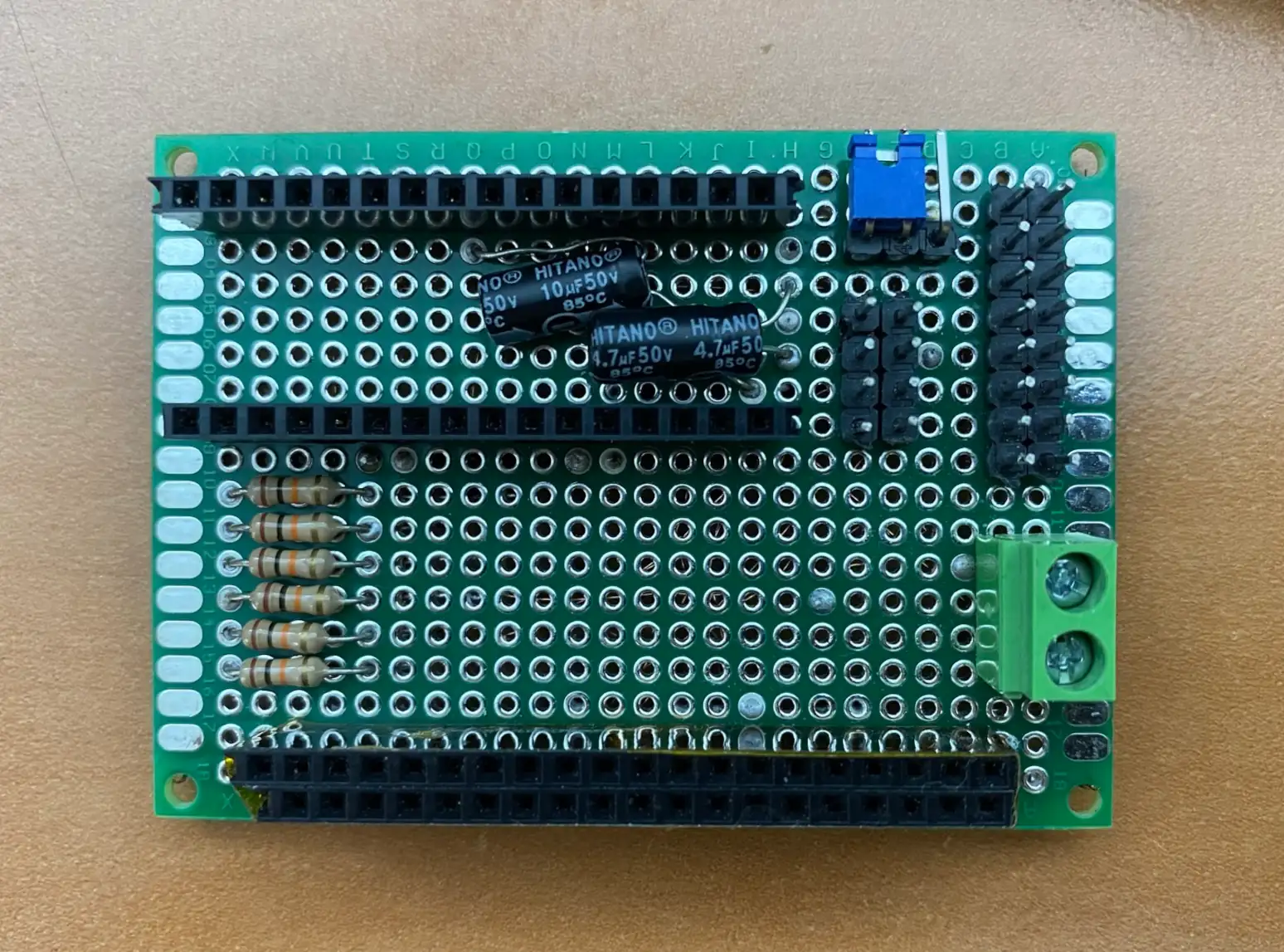
Figure 3. The finished board top-side.
It was difficult to decide how to wire up the prototype board. Using wires from an old floppy cable proved too finicky, it was easy to burn them in such an enclosed space, and they were not so easy to manoeuvre as I thought. I ended up settling for tiny pieces of enamelled copper wire cut from the winding of an inductor. The enamel (usually) burns off only on the parts that are soldered, reducing the risk that "traces" will short against each other. I learned that once it has burned off, the copper is also very easy to tin, and making a clean bond isn't really a problem for me.
Now, don't get a shock! When wiring up the SPI headers, test clips try to reproduce the pin layout of the chip on the connector-end, so the pin numbering may not be what you would expect. Try to imagine an actual SOIC-8/16 chip sitting on the board, and how the pinout would look there. You will notice that while these 2.54mm headers are normally row-major, the test clip requires an unusual U-shaped pin ordering. KiCad, for example, has no preset for this; you must re-order the pins in the footprint editor.
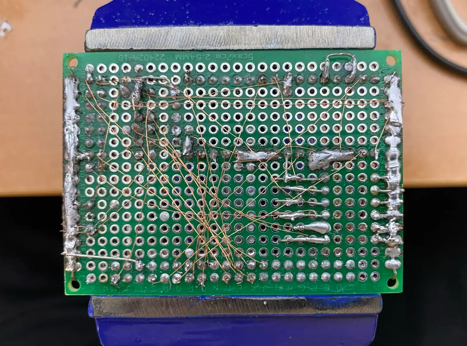
Figure 4. The finished board fully soldered (showing all connections).
As you can see, the organisation is a bit of a mess, but otherwise this is not too shabby. The pin assignments here were not so ideal, and I was more focused on wiring everything up this time around than keeping them as neat as possible. The long line of solder on the left is a common ground, and on the right, 3.3V.
Device Setup
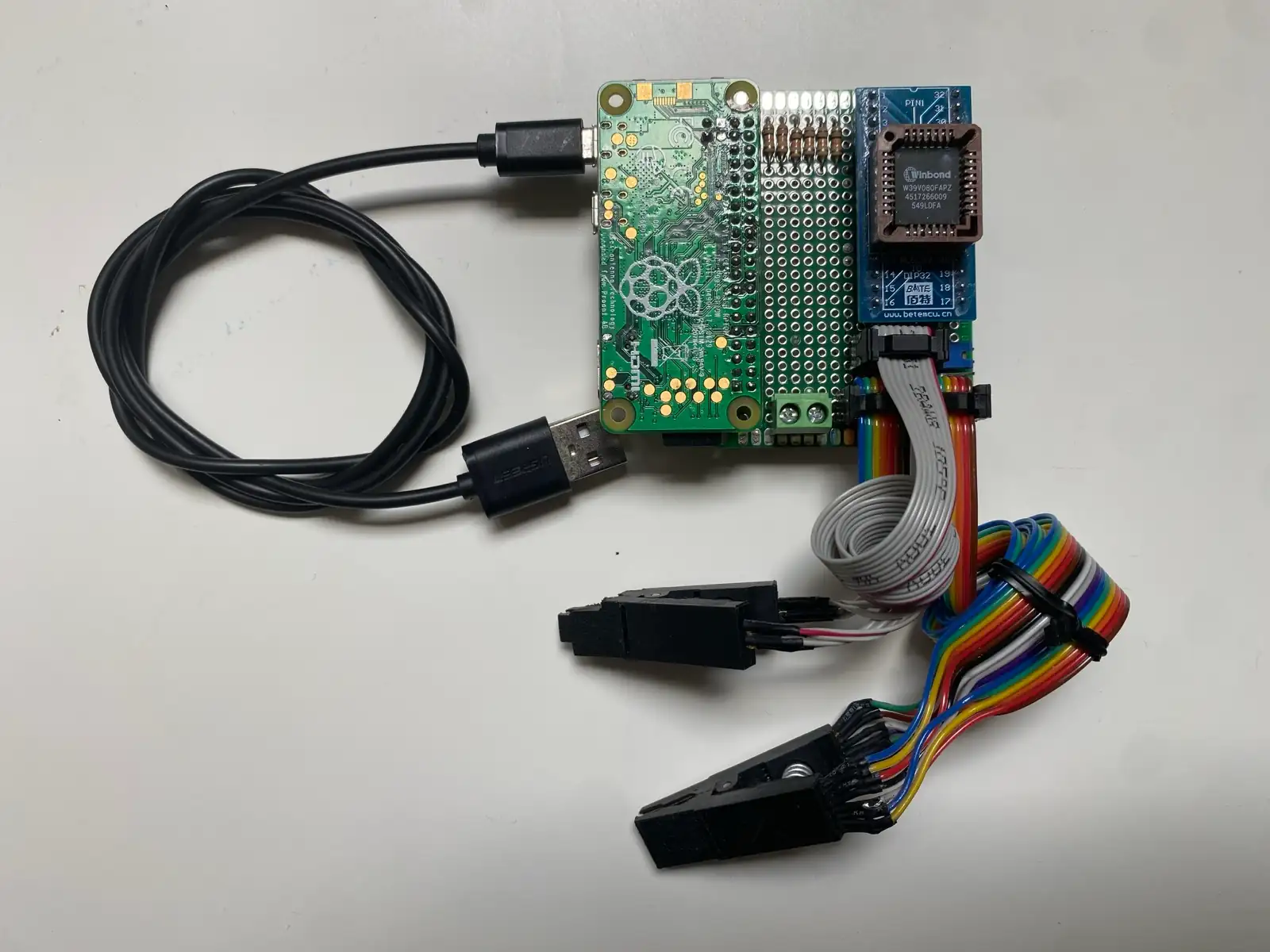
Figure 5. A photo of the finished device. This shows the orientation with which devices should be connected.
For an operating system, I used a very simple image of Alpine Linux placed onto a tiny 512 MB MicroSD card(!) and loaded this onto a Raspberry Pi Zero W. Technically, any other Raspberry Pi model should also be compatible.
Setting up Alpine Linux is a fairly intuitive process, and nothing too special has been done on my device, so I will not document it too much here.
I also used WiFi for my device and made it accessible via an SSH server on the network to run fwhtool and flashrom. This generally means less desk clutter, and I don't need to worry so much about a loss of connection if all of the flash chip images we're working with are stored on the device itself. I used the btrfs filesystem when setting up Alpine (export ROOTFS=btrfs before you run setup-alpine) in order to guarantee the integrity of the files on the card, as well. This is probably for the best, as it helps mitigate the unreliability of these devices.
Activity Indicators and More
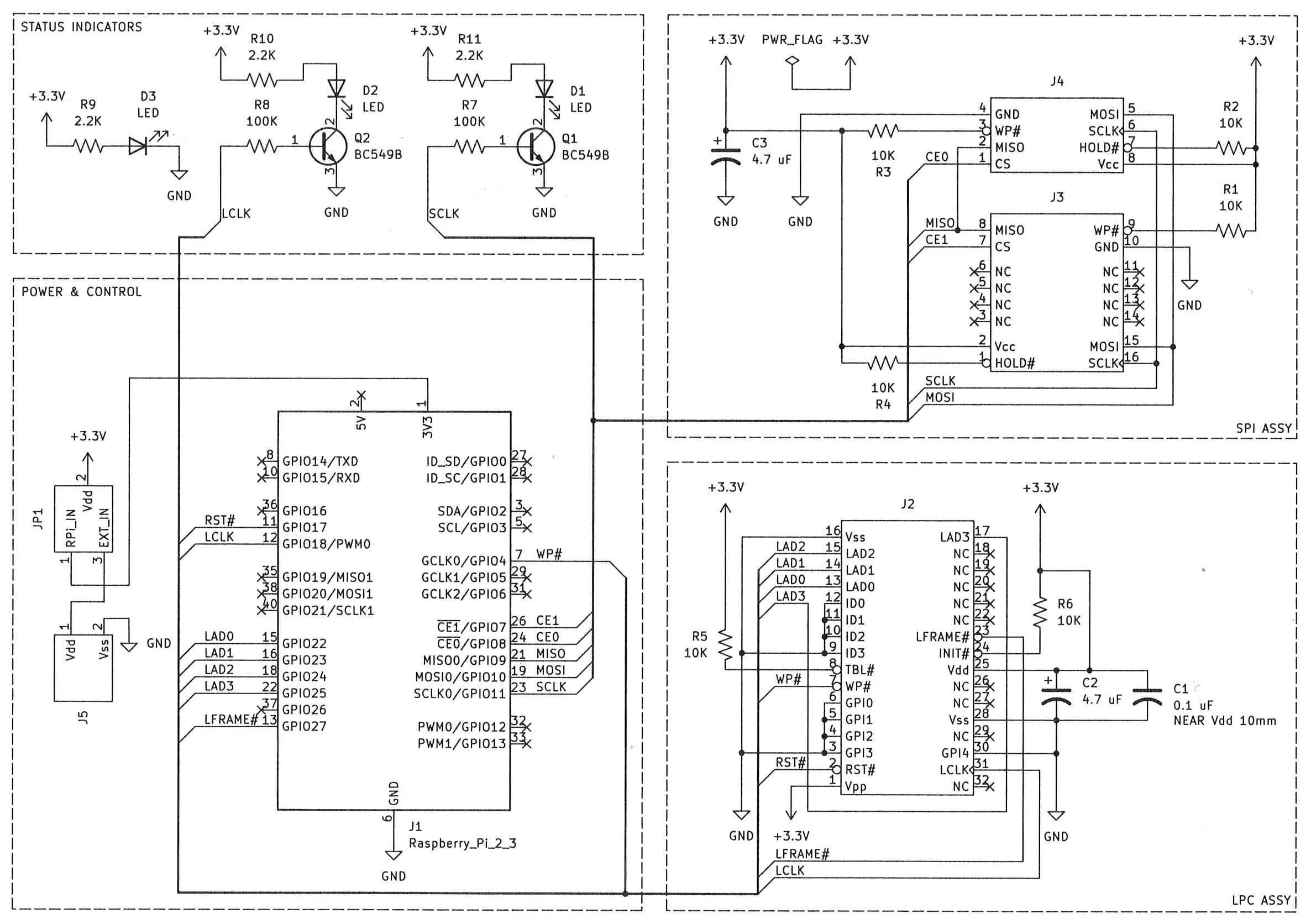
Figure 6. The second version of the schematic.
I did produce another iteration on the schematic. Most notably, this version provides an optional "status indicators" block, which uses a few bi-polar junction transistors to flash conventional green LEDs in response to LCLK/SCLK activity. There is also a power indicator, to make sure you are supplying 3.3V correctly to the common rail.
I haven't tested this iteration, but it should work. I don't have a need for it and experimented with the design mostly for fun, so I leave this up as an exercise to the reader. I may use this when producing a more polished version of the board as an actual PCB; check back here for this, because I may be selling pre-assembled versions if there is anyone who would like an easy ready-made flash programming solution for these protocols.